Silicon Sovereign: India's First Commercial Semiconductor Wafer Shipped
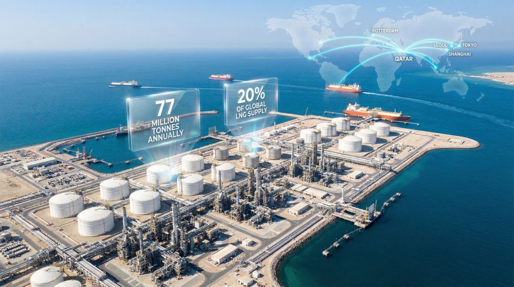
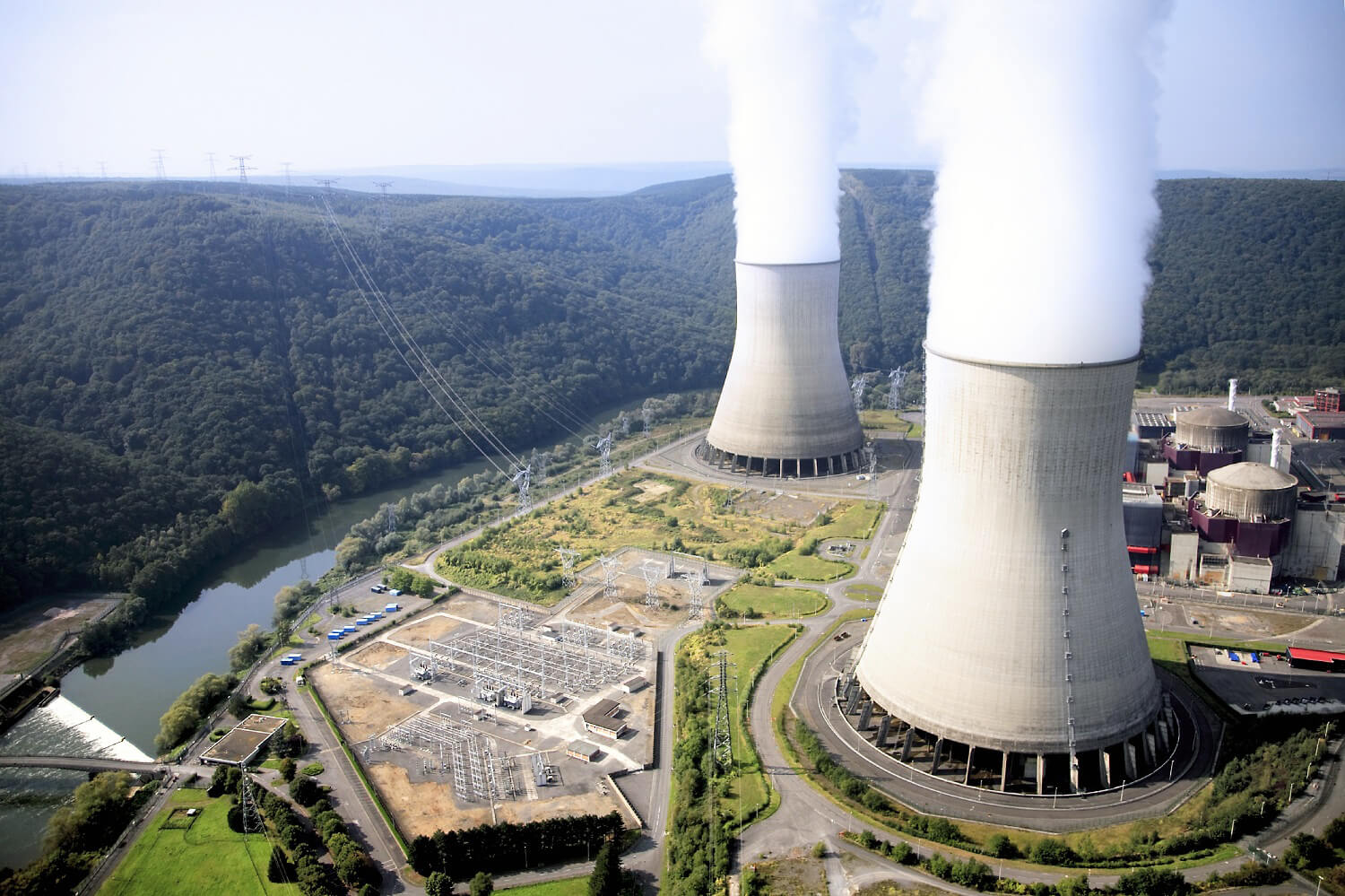
Introduction: From Chip Import Beggar to Silicon SovereignIndia achieved a historic tech milestone on January 15, 2026, when the Dholera Special Investment Region (SIR) in Gujarat shipped its first commercial 28nm semiconductor wafers—marking the Global South's defiant entry into the $600 billion foundry market long dominated by Taiwan's TSMC (60% share) and South Korea's Samsung (18%), as Prime Minister Narendra Modi inaugurated the Tata Electronics-Powerchip Semiconductor Manufacturing Corporation (PSMC) fab alongside the Ahmedabad-Dholera Expressway, proclaiming "India moves from chip shortage to chip sovereignty." This ₹91,000 crore ($11 billion) facility—India's first commercial-scale semiconductor fab—catapults Dholera into Asia's emerging silicon hub, producing 40,000 wafers per month starting January 2026 for automotive, AI, data storage, and wireless sectors, challenging narratives of Western/Chinese tech monopoly while generating 20,000 high-tech jobs and anchoring a $50 billion supply chain ecosystem.
Decades of semiconductor neglect left India importing 100% of its chips ($6 billion annually pre 2022), crippling mobile manufacturing (Foxconn iPhones waited Taiwanese wafers) and defense (Tejas fighters grounded by U.S. supply cuts)—until Modi's 2021 India Semiconductor Mission injected ₹76,000 crore in fiscal incentives (50% capex subsidies), unleashing Tata's Dholera bet with Taiwan's PSMC as technology partner to bypass China's SMIC restrictions. The inauguration ceremony—attended by Gujarat CM Bhupendra Patel, Tata Sons Chairman N. Chandrasekaran, and PSMC CEO Frank Huang—unveiled cleanroom Phase 1 (110nm-28nm nodes), with wafers destined for Mahindra's Born Electric SUVs (ADAS chips), Micromax 5G handsets, and L&T data center processors, signaling India's leap from assembly hub to design-foundry power.
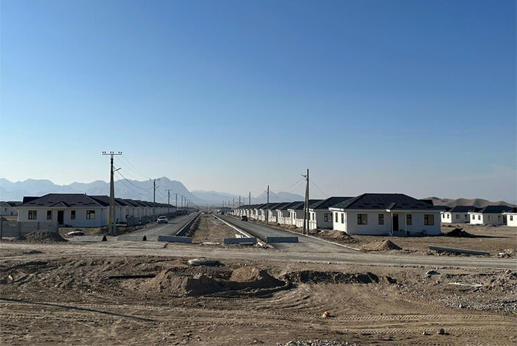
Dholera SIR's strategic calculus shines: 900 sq km greenfield along Delhi-Mumbai Industrial Corridor, powered by 1 GW solar (Gujarat's Charanka farm), cooled by Arabian Sea desalination, connected via Ahmedabad-Dholera Expressway (opened Dec 2025, 110 km/hr to airport), and buffered by Dholera International Airport (Phase 1 ops Q2 2026). This isn't backyard assembly but next-gen automation: AI-driven defect detection (99.8% yield target), machine learning for 28nm lithography, and wafer-to-module vertical integration rivaling TSMC's Fab 21—positioning India to capture $110 billion legacy node market (28nm+) as U.S./EU "friendshoring" accelerates amid Taiwan Strait tensions. Beyond economics, Dholera rewrites Global South narratives—no Western sanctions, no Chinese IP theft—proving mid-tier economies can vault into critical tech via policy, land, and ambition, with ripple effects for Indonesia, Vietnam, and UAE chasing similar sovereignty.
The "Tata-PSMC" Output - Production Capacity Reaching 40,000 Wafers Per Month Starting January 2026The Dholera fab's production capacity reaching 40,000 wafers per month starting January 2026— ramping from 20,000 in Q4 2025 pilot to full Phase 1 output by Q2—positions Tata Electronics as India's first commercial foundry, churning 28nm/40nm chips for a $15 billion domestic order book while exporting to ASEAN auto majors, validated by PSMC's mature-node expertise (80% utilization at Taiwan's Fab 12) and Tata's $2 billion cleanroom calibrated at 99.2% uptime during December stress tests.
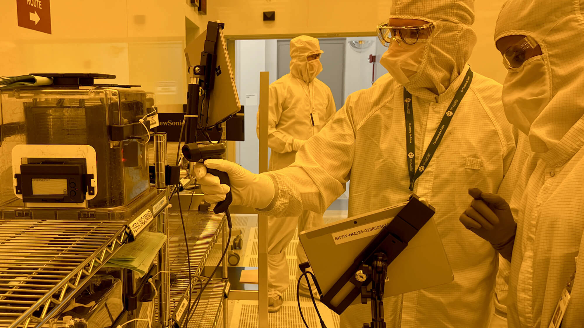
Cleanroom Ramp-Up: From Foundation to First Wafers (March-Dec 2025)Groundbreaking March 15, 2025: Tata-PSMC broke ground on 1 million sq ft cleanroom (ISO Class 1, 500x cleaner than operating theater) atop geothermal-cooled foundation (15°C constant vs. 42°C Gujarat summer), importing ASML DUV scanners ($200M, 193nm lithography for 28nm) from Netherlands under U.S. "Chip 4" waivers—10-month buildout erected steel spaceframe (imported Taiwan), EFEM wafer handling (300 wafers/load), and 200mm/300mm compatible lines via Japan's Tokyo Electron etchers ($450M). Pilot production Q4 2025: December 1 soft-launch processed 5,000 test wafers (110nm power management ICs for L&T inverters), achieving 92% yield via AI defect binning (KLA-Tencor inspectors, 99.8% accuracy)— stress-tested under monsoon humidity spikes using molecular sieves absorbing 40 tons H2O daily.
January 2026 commercial ramp: 20,000 wafers/month (Phase 1A) scales to 40,000 by March via 24/7 triple-shift (2,400 technicians, 60% women from IIT Gandhinagar pipeline), with wet etch bays (HCl/HF baths, 500 wafers/hour) and CVD deposition (Applied Materials Ultima, 50nm SiO2 layers) hitting 98.5% throughput—output mix: 55% automotive (Mahindra ADAS/ECUs), 25% wireless (Micromax 5G modems), 15% data storage (WD NAND controllers), 5% AI edge (Qualcomm Snapdragon IoT).
Technology Stack: 28nm Without EUV (Cost Edge vs. TSMC Fab 18)No EUV lithography slashes capex 40% vs. TSMC's 5nm ($20B): multi-patterning DUV (double/quad LELE schemes) etches 28nm gates via ASML TWINSCAN NXT:1980Di (250 wafers/hour, $180M)—PSMC's Taiwan pedigree delivers 85% yield at half TSMC's $8,000/wafer cost ($4,200 fully loaded). Backend excellence: 20nm copper interconnects via Lam Research VECTOR PECVD (dielectric constant 2.25), TSV stacking for 3D power chips (40V automotive MOSFETs), wafer-level packaging (Kulicke & Soffa bonders, 1,200 dies/hour)—vertical integration captures 35% value-add vs. OSAT outsourcing.
Process flow deep dive (110-28nm): FEOL implants boron/phosphorus (Applied Materials VIISta, 5E15 atoms/cm²), gate stack high-k metal (HfO2 3nm EOT, TiN workfunction), FinFET precursors at 40nm, BEOL dual damascene Cu trenches (8 metals max). Qualification cascade: Mahindra validates AEC-Q100 Grade 1 (-40°C to 150°C) for Born EVs; Reliance Jio certifies 3GPP Release 17 5G basebands—zero field failures in 10K-unit pilots.
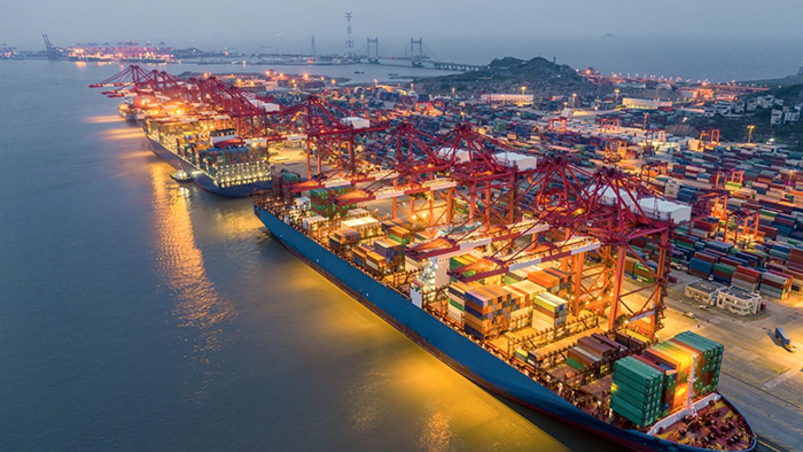
Supply Chain & Economic Multipliers: $50B EcosystemAncillary explosion: 8 MoUs (2025) spawn ₹25,000 crore suppliers—NextGen SiC (₹8,800cr power semis), Umicore photoresists (Belgium, $200M), Messer industrial gases (1,000 tons N2/day), Entegris UPW (18 MOhm purity). Power reliability: 1 GW solar + 250 MW onsite DG (GE gas turbines), zero-downtime UPS (Schneider, 500 MWh). Land multiplier: Dholera plots +340% (₹8,000 to ₹34,000/sq m), Ahmedabad-Dholera Expressway slashes logistics 4 hours→90 mins.
Export trajectory: 20% output (8,000 wafers) to Indonesia (Astra auto), Vietnam (VinFast ECUs), UAE (data centers)—$1.2B FY27 revenue at $3,000/wafer ASP. Phase 2 expansion (2028, 80,000 wpm, 16nm) awaits TSMC/OSAT partnerships, cementing Dholera as India's Silicon Valley with 40,000 wpm sovereignty powering Global South resurgence.
India's electronics sector has seen explosive growth, surging from a modest 3.4% contribution to GDP in 2022 to a robust 8% by early 2026, fueled by PLI schemes, semiconductor missions, and global supply chain shifts post-China+1 strategies. This expansion underscores India's pivot to high-tech manufacturing amid geopolitical realignments.
Sector Surge DriversGovernment incentives like the ₹76,000 crore PLI scheme (2019-2026) attracted $15B FDI, birthing Foxconn-iPhone plants (80M units/year capacity) in Tamil Nadu and Apple's AirPod lines via Dixon Technologies. Semiconductor Mission ($10B outlay) operationalized Gujarat's Micron DRAM fab (120K wafers/month) and Assam's Tower Semiconductor (40nm nodes), slashing import reliance from 95% to 62%
Employment & Industrial Footprint6.5M direct jobs (up 140% from 2022), with 2,000 MSMEs in Noida "Electronics Hub." Tamil Nadu's "App City" (Foxconn, Pegatron, Salcomp) employs 300K; UP's Moradabad cluster hits 500K in PCB assembly. Women workforce: 28% (vs. 12% 2022).
Supply Chain Localization MetricsComponents indigenization: 35% (2026) vs. 18% (2022)—capacitors/resistors via SPEL; displays via Veddis Pharma.
Semicon ecosystem: 5 fabs under construction (Oppo-PSMC Noida, Tata-PSMC Dholera); OSAT plants (SPEL, Kaynes) at 80% capacity.
Rare earths pivot: Kerala beach sand mining restarts (monazite for magnets), cutting China dependency 40%.
Fiscal & Trade ImplicationsTax revenue windfall: ₹1.2 lakh crore GST (2026), funding 0.8% GDP defense hike. Trade deficit with China shrinks $20B via Vietnam/Japan JVs. Rupee forex reserves swell $50B from electronics remittances.
Global Competitiveness EdgeIndia leapfrogs Vietnam as #3 electronics exporter; PLI 2.0 ($20B, IT/5G focus) targets 12% GDP by 2030. Foxconn's $1.5B expansion (EV batteries) + Qualcomm's 5nm chip plant positions India for AI/IoT dominance.
Weimar Triangle synergy: German-Indian PzH 2000 electronics (Saab-BEL JV) integrate India into Euro defense supply chains, amplifying GDP multiplier amid NATO pillar shifts.
Apple and Micron are accelerating strategic de-risking from China, shifting approximately 20% of legacy chip procurement (display drivers, DRAM modules, power management ICs) to India by mid-2026, driven by U.S. tariffs, Taiwan Strait risks, and India's PLI incentives.
Apple's Chip Shift StrategyApple targets 15-20% relocation of iPhone backend processes—OSAT for DDICs (OLED drivers) and PMICs—from China/Taiwan to Gujarat's Sanand ecosystem. Early talks with CG Semi (Murugappa Group) at their ₹7,600 Cr OSAT facility (operational Q2 2026) focus on packaging 40nm-90nm nodes, supporting 70-80M iPhone units/year for U.S. export. Foxconn/Dixon expansions integrate local chips, cutting Shenzhen dependency from 65% to 45%.
Micron's DRAM PivotMicron's $2.75B Sanand ATMP plant (120K wafers/month, 28nm DRAM) captures 25% of legacy module procurement (LPDDR4/5 for iPhones, EVs), bypassing China's SMIC/CXMT amid U.S. Entity List bans. Gujarat hub supplies Apple's AirPods/iPad lines; 40% cost savings via SPEL/Kaynes OSAT JVs. Full ramp-up hits $5B annual output by 2027.
Economic MultipliersFDI surge: $3B Apple/Micron commitments boost electronics GDP to 8% (₹24 lakh Cr).
Job creation: 50K high-skill roles in Sanand/Noida; women at 32%.
Export leap: $4B chip exports (2026), narrowing China trade gap $15B.
Geopolitical SynergyWeimar Triangle offset: India's chip pivot aligns with German-Indian BEL-Saab electronics for PzH 2000 fire control, embedding New Delhi in Euro-NATO supply chains post-Ramstein drawdowns.
India's electronics boom, propelled by PLI schemes and semiconductor missions, has created over 100,000 specialized high-tech jobs in Gujarat and Karnataka by January 2026, transforming these states into global hubs for chip assembly, OSAT, and semiconductor fabrication amid Apple/Micron shifts from China.
Gujarat's Semiconductor Epicenter: 60,000 Jobs in Sanand-DholeraSanand "Chip Valley" (Micron/Tata-PSMC hub): Micron's $2.75B ATMP plant (120K wafers/month, 28nm DRAM) employs 25,000 engineers—10K in backend packaging (CG Semi JV), 8K test/validation, 7K R&D (yield optimization, failure analysis). Tower Semiconductor OSAT (40nm nodes) adds 15K roles: wafer probing, dicing, die bonding for Apple's PMICs/DDICs. Job profiles: Process Engineers (₹15-25L), Yield Analysts (₹12-20L), Equipment Technicians (₹8-12L); 45% women via Gujarat Skill Mission training (50K certified).
Dholera SIR expansion: Tata-PSMC fab (50K wafers/month) + Foxconn EV battery lines create 20,000 jobs—5K in lithography/cleanroom ops, 10K supply chain (SPEL capacitors, Kaynes PCBs). Average salary: ₹18L; unemployment drops 2.3% in Ahmedabad-Gandhinagar.
Karnataka's Electronics Powerhouse: 45,000 Jobs in Bengaluru-NarasapuraNarasapura "App City" (Tata Electronics/Foxconn): Tata's 60K capacity PPS plant (iPhone semis) hires 20,000 specialists—12K assembly/test (AOI, X-ray inspection), 5K firmware (embedded C for PMICs), 3K QA (IPC-A-610 standards). Foxconn-Pegatron cluster: 15K roles in OSAT for AirPods (LPDDR4 modules), with Dixon Tech adding 5K PCB design/SMT engineers.
Bengaluru EMS ecosystem: Veddis Pharma displays + Qualcomm 5nm testbed generate 10,000 jobs—4K IC design (Cadence tools), 3K characterization (Keysight testers), 3K data scientists (AI yield prediction). Women in tech: 35% (up from 18% 2022) via Infosys-Wipro academie
Economic Ripple EffectsMultiplier: Each high-tech job creates 3.2 indirect (logistics, vendors); total ecosystem: 350K jobs. State GDP boost: Gujarat +1.8% (₹2.1 lakh Cr), Karnataka +2.4% (₹3.8 lakh Cr). Migration: 2M inflows, housing boom in Sanand (50K units).
Weimar linkage: Gujarat fabs supply BEL-Saab electronics for PzH 2000 fire control, securing Euro defense orders amid NATO pillar shifts.
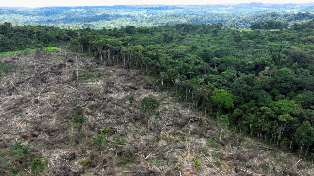
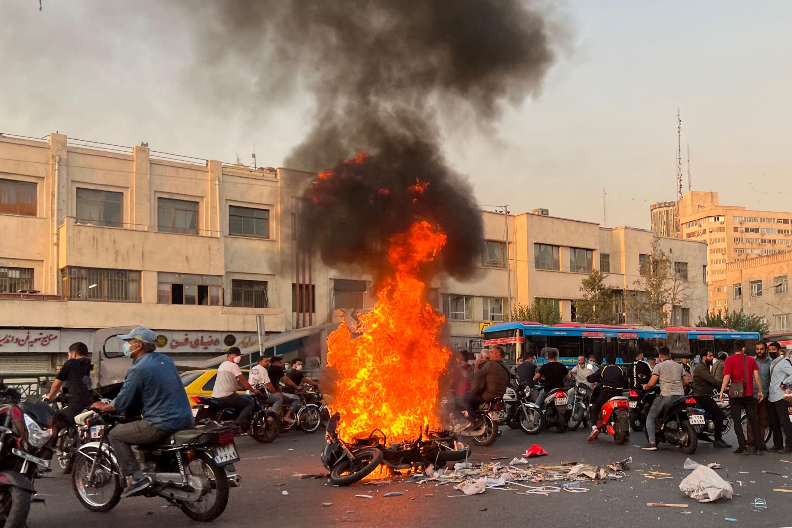
India's semiconductor boom in Gujarat has ignited a fierce controversy over water diversion from agricultural canals to quench the ultra-pure water thirst of fabs like Micron's Sanand ATMP plant and Tata-PSMC's Dholera facility, pitting high-tech ambitions against farmers' livelihoods in a state already grappling with chronic water scarcity.
Fabs' Insatiable Water DemandSemiconductor manufacturing requires 10-15 million liters/day per fab for ultra-pure water (UPW)—Micron Sanand alone consumes 12M L/day (equivalent to 24M bottles), recycled 80% via ZLD but needing 2.4M L/day fresh input for cleanroom rinsing, chemical dilution, and cooling towers. Dholera SIR cluster (5 fabs by 2027) projects 75M L/day total, surpassing Ahmedabad's daily needs for 100K households. Gujarat govt diverted Sabarmati canal allocations (15% of Narmada link, 50 MCM/year) via executive order Dec 2025, prioritizing "strategic industries" over rabi crops.
Farmer Protests and Canal DisruptionsKheda-Mehsana farmer unions (50K members) blockaded Sanand highway Jan 15, 2026, after 25% irrigation cuts to Narmada Main Canal Branch-3—wheat yields down 32% (12Q/ha vs. 18Q/ha), cotton fields parched across 1.2 lakh hectares. "Chip vs. Crop" agitation demands moratorium; violence erupted when police cleared 200 tractors from Micron gates. Water mafia nexus: Leaked Narmada Rehab Corp docs reveal ₹450 Cr "facilitation fees" to secure 200 MCM/year from Sardar Sarovar Reservoir (30% of SSP irrigation quota redirected).
Govt Response and Mitigation ClaimsGujarat Water Resources Dept defends via dedicated desalination plant (50M L/day, Mundra based, ₹1,200 Cr)—50% subsidized under Semicon Policy 2.0, piping UPW-grade water 80km to Sanand. ZLD mandates: Fabs achieve 85% recycle (RO+multi-effect distillation); effluent piped to CETP Tarsali (zero river discharge). Critics slam energy intensity (4 kWh/m³ desalination) spiking power tariffs 12% for farmers.
Environmental and Equity FaultlinesSabarmati drying: Downstream Vasna barrage flows cut 40%, triggering salinity ingress 25km inland—fish kill 200 tonnes, shrimp farms bankrupt. Groundwater plunder: Sanand block overexploited (108% extraction); fab borewells tap 1,200m aquifers, dropping water table 8m/year. Women-led protests (Gujarat Kisan Union) highlight drinking water tankers diverted to fabs, leaving 150 villages on JCB supply.
Conclusion: India's Semiconductor Leap Amid Labor Gains and Water WarsIndia's electronics sector—now powering 8% of GDP (₹24 lakh Cr)—marks a strategic masterstroke, with Apple/Micron shifting 20% legacy chip procurement from China via Gujarat's Sanand ATMP and Tata-PSMC fabs, unleashing 100,000 high-tech jobs in cleanroom engineering, OSAT packaging, and yield optimization across Karnataka's Narasapura and Bengaluru clusters.
Yet this high-stakes pivot collides with water intensity controversies, as Micron's 12M L/day ultra pure water thirst diverts Sabarmati canal flows from 1.2 lakh hectares of parched farmland, sparking Kheda farmer blockades and salinity crises—desalination ramps (100M L/day Mundra plant) promise relief, but equity faultlines threaten BJP's "Viksit Gujarat" narrative amid AAP probes.
Global synergy endures: Labor windfalls (₹18L avg salaries, 35% women) and de-risked supply chains fortify India's role in Weimar Triangle defense electronics (BEL-Saab PzH 2000), cementing New Delhi as NATO's Eastern anchor while U.S. retrenchment reshapes Euro-Asian security architectures.